Semiconductor
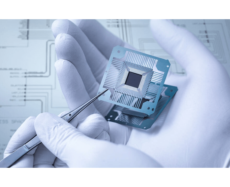
High Performance Semiconductor Components
As chips become smaller and denser, more stringent requirements in the fabrication environment have spurred development of higher performance semiconductor equipment components. This requires more sophisticated processes and fabrication equipment from component manufacturers like Elcon Precision.
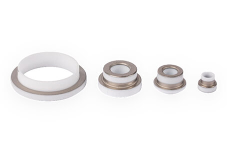
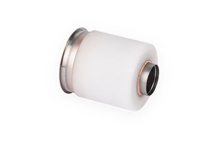
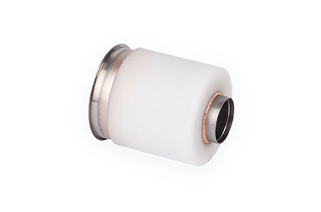
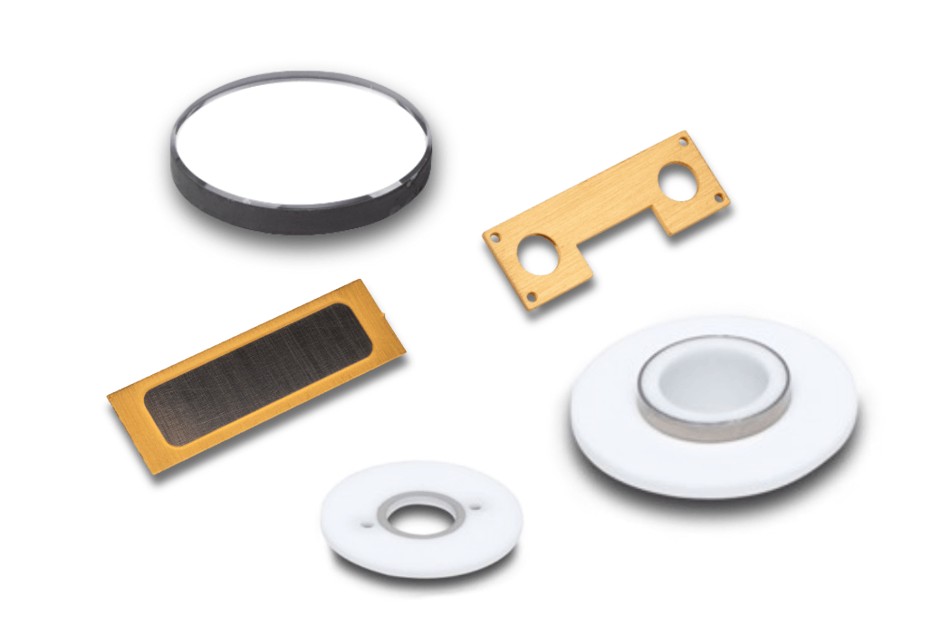
Improvements in advanced process techniques developed at Elcon Precision have expanded our expertise in bonding ceramics, screen printing metallization, photoetching copper and refractory metals, and brazing hermetic feedthroughs. Customers come to us for critical components such as high voltage devices, metallized lift pins and multizone electrostatic chuck circuitry.
As semiconductors become smaller and denser, Elcon's capabilities provide precision components that satisfy stringent requirements for the latest technologies.
Semiconductor Applications
| Application | Benefits |
|
High hermiticity |
|
Multizone, thinner, very durable |
|
Multizone thick film metallization |
|
High volume, high pitch count |
|
Low set-up costs, bend lines at no additional cost, in-house forming |
|
Burr free, stress free, metal properties preserved |
|
Uniform thickness, thermal uniformity |
Frequently requested services
- Photochemical Machining
- Screen print metallization
- Mo-Mn metallization
- Tungsten metallization
- Mo-Mn-W Metallization
- Ceramic-to-metal brazing
Advanced finishing services
- Precision grinding and lapping
- CNC machining
- Plating
- Specialized coatings